Central Technology Facility for Research and Development
The Instrumental Research and Development group, within the Laboratory for the Study of the Universe and eXtreme Phenomena (LUX), at the Paris Observatory, operates a Central Technology Facility for Research and Development (CTRD) along with a cleanroom that is part of both the Paris local cleanroom network and the national RENATCH+ network.
The CTRD contributes to the development of new sensors, particularly superconducting ones, and micro-devices for astronomical applications. It brings together nano- and microfabrication capabilities, including a 40 m² cleanroom, a micro-assembly room, a dicing room, and a cryogenic testing laboratory. The expertise developed for astronomy can be applied to any other field (medical, industrial, etc.).
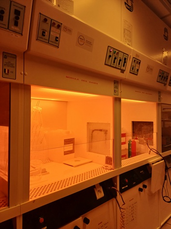
The ISO 7 class cleanroom is divided into two zones:
- a zone housing a magnetron sputtering deposition system, a cathodic evaporation system, and a RIE etching system;
- an actinic-free zone dedicated to photolithographic processes, equipped with 4 ISO 5 class laminar flow hoods.
The cleanroom is adjacent to a 30 m² grey room housing two additional deposition systems (a sputtering system and an evaporation system).
This facility is accessible to all staff from the Paris Observatory laboratories, and is also open to external companies or institutions upon request.
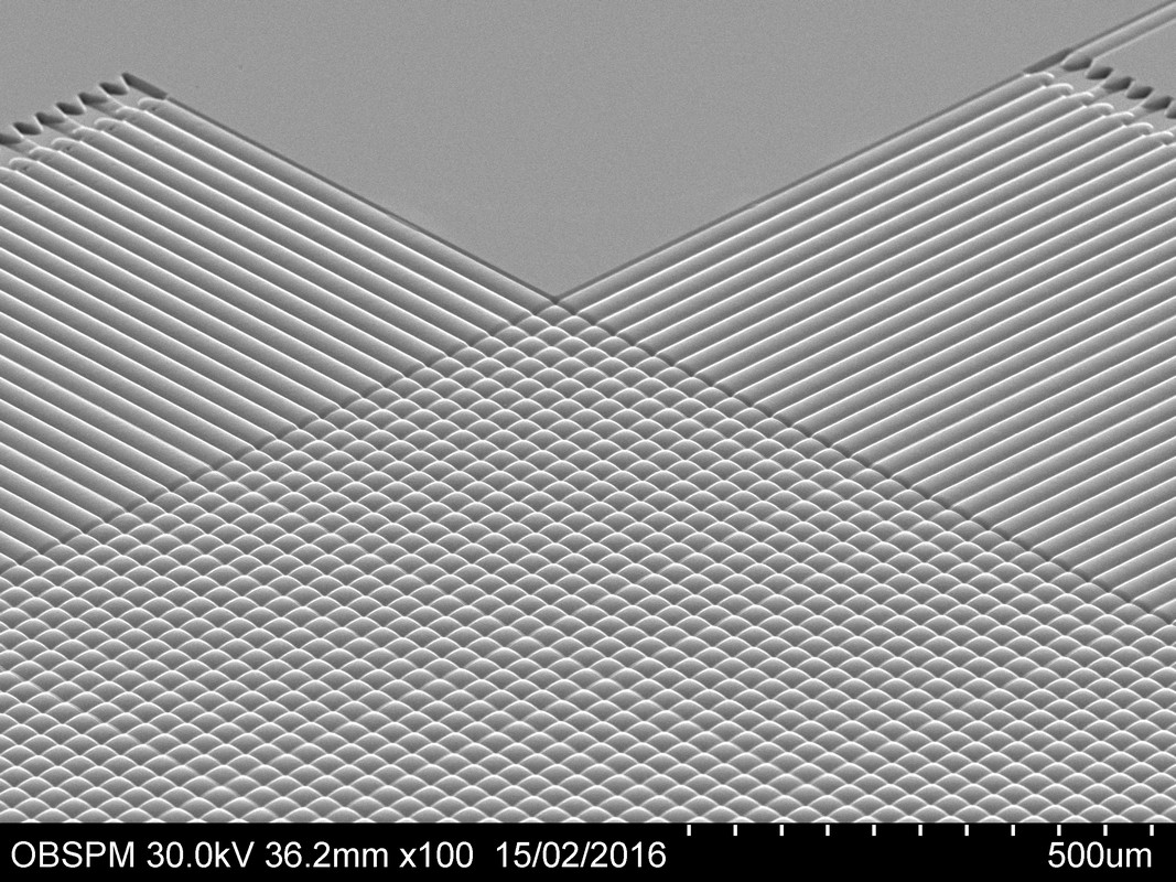
Here are the various pieces of equipment used in our technology facility.
Thin film deposition
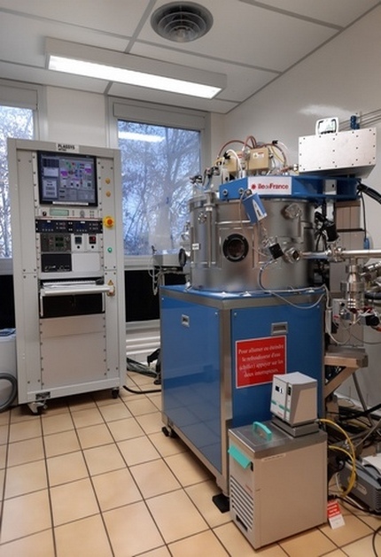
Bâti Plassys MP700S
• Taille des wafers: 100mm
• Gaz de process: Ar, N2, O2
• Cibles disponibles: Au, Ti, Al
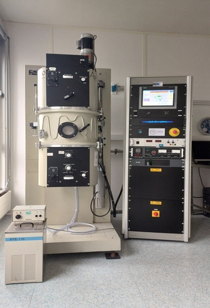
Bâti Phénix
• Taille des wafers: 50mm
• Gaz de process: Ar, N2, O2
• Cibles disponibles: Al, Nb, NbTi
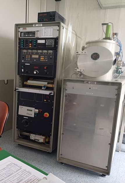
Bâti d'évaporation non diélectriques
Matériaux: Au, Cr, MgF2
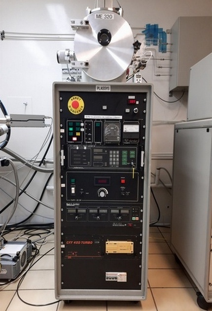
Bâti d'évaporation diélectriques
Matériau: SiO2
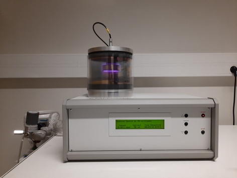
Dépôt d'or par plasma
Description...
Thin film etching
Bâti de gravure RIE
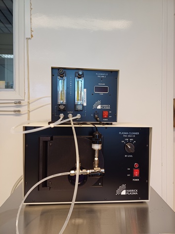
Cleaner plasma à oxygène
Photolithography
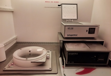
Modules de chimie (acides, bases, solvants, enduction de résine photosensible)
Modules de chimie (acides, bases, solvants, enduction de résine photosensible)
Tournette & Plaque chauffante
Tournette & Plaque chauffante
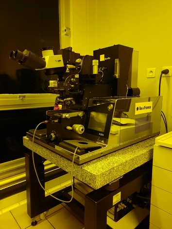
Machine d'alignement et d'insolation MJB4 (UV3, UV4)
Machine d'alignement et d'insolation MJB4 (UV3, UV4)
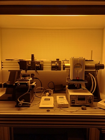
Banc d'insolation de trames de microlentilles
Banc d'insolation de trames de microlentilles
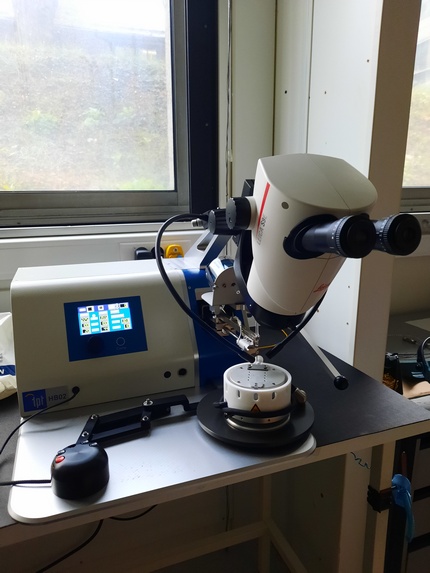
Characterisation
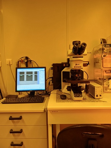
Microscope optique OLYMPUS
Microscope optique OLYMPUS
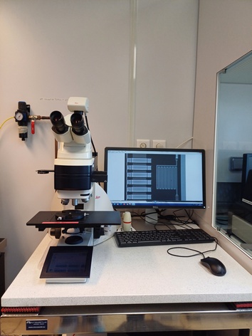
Microscope optique LEICA
Microscope optique LEICA
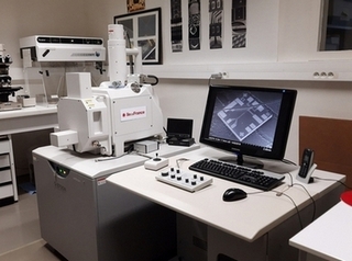
Microscope électronique à balayage HITACHI
Microscope électronique à balayage HITACHI
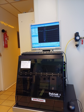
Profilomètre mécanique BRUKER
Profilomètre mécanique BRUKER
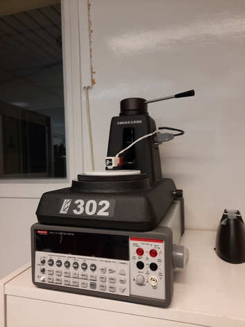
Résistivimètre 4 pointes
Résistivimètre 4 pointes
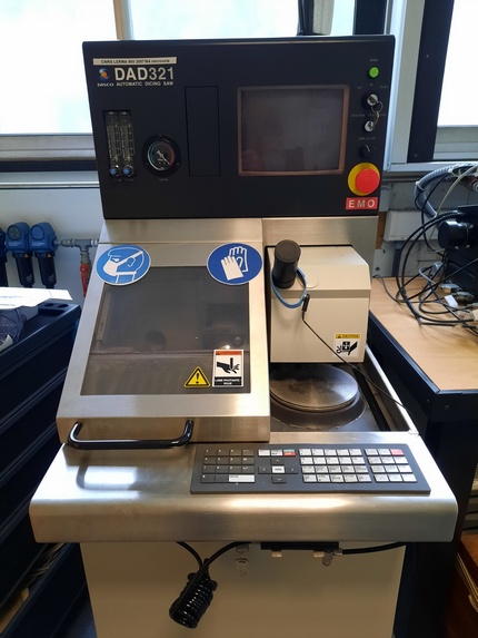
Dicing and component assembly
Découpe
Scie DAD 321
Montage
Machine de micromontage bonding
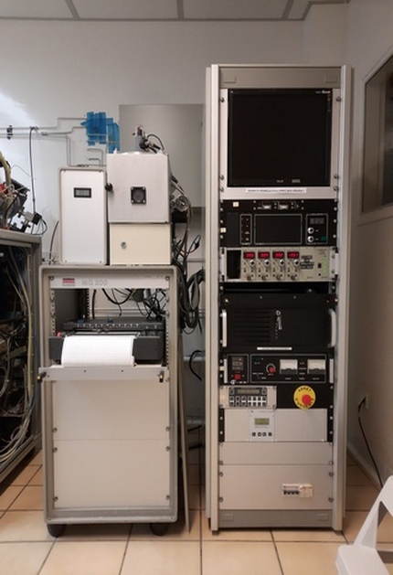
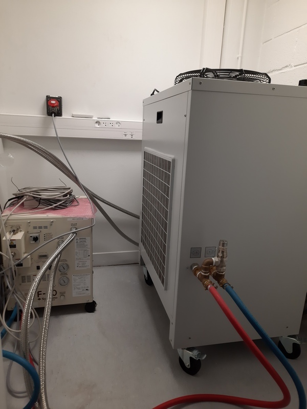
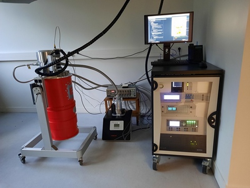
Cryogenic measurements
Cryostat 300mK
Cryostat 300mK
Compresseur à hélium, chiller
Compresseur à hélium, chiller
Mesures de températures critiques
Mesures de températures critiques
Achievements
Selected achievements
Projects that showcase our expertise
Détecteurs KIDs
Kinetic Inductance Detectors (KIDs) are based on measuring the change in kinetic inductance caused by photon absorption in a thin strip of superconducting material. The change in inductance is typically measured as a shift in the resonant frequency of a microwave resonator. These detectors are also known as Microwave Kinetic Inductance Detectors (MKIDs).
They represent a leading cryogenic detection technology for millimetre-wave astrophysics, thanks to their sensitivity and ability to be assembled into large arrays. These detectors use frequency-domain multiplexing, enabling the readout of thousands of pixels over a single coaxial cable.
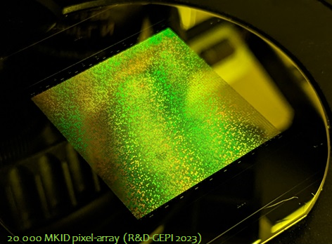
The image below shows a 20,000-pixel array produced for the ERC-funded project SPIAKID, using MKID technology.
Fig.1 20,000 pixel MKID detector array
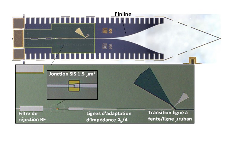
SIS junctions
SIS junction
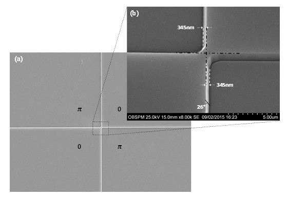
Coronography
Four-quadrant phase mask
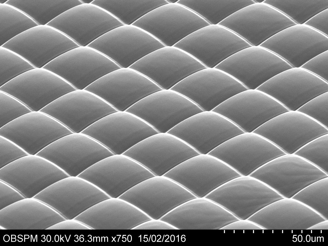
Microlenses
Contact
Contact
To reach us, send an email to the following adress: